This page presents a summary description of the main components of Logisim that you will need for the first design office session and the first laboratory session.
1. Register

This is a classic edge-triggered register, whose size is indicated via the Bit Width attribute.
1.1 Basic Operation
The register's value is continuously output on the {$Q$} output. To store a new value, it must be presented on the {$D$} input and an ascending edge must be sent to the clock command (small triangle at the bottom).
In basic operation, do not connect anything to {$clr$}.
During simulation, it is possible to manually enter a value into the register. To do this, click on it with the interaction tool, then type a value in hexadecimal.
1.2 More Information
The register's value is forced to 0 if a signal of 1 is present on the {$clr$} command.
2. RAM
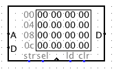
The RAM component in Logisim is a read-write memory. You can specify the size of the memory words (Data Bit Width attribute) as well as the size of the addresses (and therefore the size of the memory, Address Bit Width attribute).
2.1 Basic Operation
The memory can provide values located at an address, or write values to that address. The address must be specified continuously on the {$A$} input. Note that if {$A$} changes, the address pointed to by the memory changes immediately: there is no address memorization. To memorize the address, it may be useful to add a memory address register ({$MAR$}) upstream of the {$A$} input.
Reading. To operate the memory in read mode, set the ld port to 1. Then, the read data is available on the {$D$} port on the right side of the memory.
Writing. To write data to memory, present that data on the {$D$} port on the left side, while applying a value of 1 to the {$str$} port. The memorization is performed when an ascending edge is sent to the clock input (small triangle at the bottom).
Important. Make sure that the value imposed on the ld port is always the inverse of the value on {$str$}.
It is not necessary to connect the sel and clr ports.
2.2 Advanced Operation
The clr port allows you to set the entire memory to zero (apply a value of 1).
The sel port allows you to disable the memory (by applying a value of 0), effectively disconnecting it.
2.3 Memory Content Manipulation
Right-clicking on a memory component opens a context menu allowing you to manipulate its contents:
- Edit Contents: Opens a window allowing you to modify the memory content;
- Clear Contents: Sets the memory to zero;
- Load/Save Image: Allows you to load and save the memory content to a file.
3. ALU
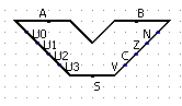
The ALU component (Arithmetic and Logic Unit) is purely combinational; it performs various operations on two inputs {$A$} and {$B$} whose bit size can be specified. The result will be available on the output port {$S$}.
The operation performed by the ALU is indicated by the four control bits {$U0$}...{$U3$}. The following table shows the operations that the ALU can perform and the corresponding values of the control bits.
| U3 | U2 | U1 | U0 | Operation |
|---|---|---|---|---|
| 0 | 0 | 0 | 0 | S = A |
| 0 | 0 | 0 | 1 | S = A or B |
| 0 | 0 | 1 | 0 | S = not (A or B) |
| 0 | 0 | 1 | 1 | S = not (A and B) |
| 0 | 1 | 0 | 0 | S = A and B |
| 0 | 1 | 0 | 1 | S = B |
| 0 | 1 | 1 | 0 | S = not B |
| 0 | 1 | 1 | 1 | S = A xor B |
| 1 | 0 | 0 | 0 | S = A - B |
| 1 | 0 | 0 | 1 | S = A + B |
| 1 | 0 | 1 | 0 | S = A + A |
| 1 | 0 | 1 | 1 | S = A - 1 |
| 1 | 1 | 0 | 0 | S = A + 1 |
| 1 | 1 | 0 | 1 | S = FFFF |
| 1 | 1 | 1 | 0 | S = 0 |
| 1 | 1 | 1 | 1 | S = not A |
On the output, the ALU has four indicators:
- {$N$}: Sign indicator, equals 1 if {$S$} < 0;
- {$Z$}: Zero result indicator, equals 1 if {$S$} = 0;
- {$C$}: Carry indicator, equals 1 if a carry appears during the calculation of {$S$};
- {$V$}: Overflow indicator, equals 1 if the calculation of {$S$} produces an overflow.
4. Control Unit
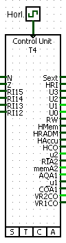
The sequencer performs two complementary functions:
- Generation of clock signals internally (synchronous circuit, fixed);
- Implementation of a purely combinational circuit defined by logical equations. These equations must be entered in a dedicated window.
4.1 Clock Signal Generation
The clock module generates signals {$T_i$} and {$P_i$} as shown below. Note that in reality, these signals can easily be generated by a set of D flip-flops connected to each other.
These signals are derived from the clock of Logisim. Therefore, a standard clock component must imperatively be connected to the input of the sequencer (top connector, triangle-shaped).
The number of time steps must be specified (attribute "Cycle Length"). After the last time step, the clock unit restarts at time 1.
The evolution of these clock signals can follow different modes which must be selected by clicking in simulation mode on one of the buttons located at the bottom of the sequencer component ({$P$}, {$T$}, {$C$}, {$A$}). Initially, the sequencer is stopped.
- Step by Step ({$S$} for "Step"). The sequencer advances by one-third of a time step (e.g., from {$T_1$} to {$T_1+P_1$}), then stops.
- Time by Time ({$T$}). The sequencer advances by one time step (e.g., from {$T_1$} to {$T_2$}), then stops.
- Cycle by Cycle ({$C$}). The sequencer advances by one cycle and stops at the beginning of the next cycle (i.e., on {$T_1$}).
- Automatic ({$A$}). Continuous operation.
In the sequencer context menu (right-click), the "Reset" option allows you to restart from the beginning of {$T_1$}.
4.2 Calculating Outputs
The combinational behavior of the sequencer is defined by a set of equations to be entered in the window provided for this purpose, which opens when you click on the text "click to edit" of the "Equations" attribute of the sequencer.
In this window, you essentially indicate what the inputs are, what the outputs are, and express the outputs as a function of the inputs and the internal signals {$T_i$}/{$P_i$}. For convenience, it is also possible to define other internal signals, in order to factorize the calculation of certain formulas.
The syntax to use for the equations is as follows:
- Line of the type "input name": defines an input;
- Line of the type "internal name = equation": defines an internal signal by providing an equation, in which the inputs, the {$T_i$}/{$P_i$} and other internal signals defined earlier in the window may appear;
- Line of the type "output name = equation": defines an output by providing an equation, in which the inputs, the {$T_i$}/{$P_i$} and internal signals may appear;
- You can use the constants 0 and 1 in the equations;
- On a line, if a # appears, the rest of the line is ignored (comment);
- Spaces are not significant;
- Empty lines are ignored.
- Logical operators are written as follows:
- & and * are used interchangeably to write a logical AND.
- | and + are used interchangeably to write a logical OR.
- ! is used to write a logical NOT.
The sequencer accepts any well-parenthesized expression. The operators are thus ordered by decreasing order of priorities: ! > & > |.
At any time, it is possible to modify the equations. As soon as the window is validated by "Ok", the values of the sequencer outputs are immediately updated.
The sequencer displays on its pins the name of the inputs and outputs that have been assigned to them. The inputs appear on the left; the outputs on the right. The pins appear in the order in which they are specified in the list of equations. If you have placed the sequencer in a diagram and you modify the equations, be sure to keep the same order for the signals, otherwise you will have to modify your wiring.
4.3 Sequencer Error States
When the sequencer is operating normally, it displays the word "Control Unit" in black at the top. If it has detected an error, red text is displayed, indicating the type of error that occurred. The errors are as follows:
- Seq#E/S: error during loading of equations.
- Seq#PARSE: syntax error in the equations: the program could not interpret one of the lines.
- Seq#EVAL: error during evaluation of the equations, generally due to the use in an equation of a signal that has not been defined.
Clicking on the sequencer with the interaction tool allows you to display a detailed error message.
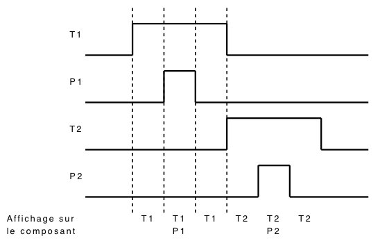
4.4 Example of Using the Sequencer
This section presents a simple example of using the sequencer, not to build a computer, but a small synchronous system. The purpose of this system is to make a register count from 0 to 9, then restart at 0, and so on. We build the following circuit, composed of a register, an ALU and a sequencer:
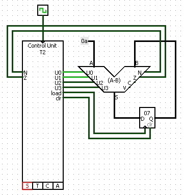
The sequencer follows cycles of two time steps; its operation is as follows:
- At time 1, the ALU adds 1 to the content of the register. The new value is loaded into the register on the rising edge of {$P_1$};
- At time 2, the ALU compares the content of the register and the number 10. If the first is greater than or equal to 10, then the register is reset to zero.
The list of equations for the sequencer is as follows:
input N
input Z
internal negative_or_null = Z | N
output U0 = 1
output U1 = T2
output U2 = T1
output U3 = 0
output load = P1
output clr = P2 & negative_or_null
5. Register File
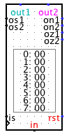
The Register File is a collection of {$n$} registers, identified by the integers 0, 1, ..., {$n-1$}. To specify the number {$n$} of registers, you must change the value of the Selector bits attribute to {$\log_2 n$}. To specify the size of the registers, you must change the value of the Data bits attribute.
The Register File has two outputs, out1 and out2, and five inputs:
- in : The data to be stored in a register.
- is : The identifier of the register in which the input data must be stored.
- rst : Destroys the contents of the registers (you can ignore it).
- os1 : The identifier of the register whose value is imposed on the out1 output.
- os2 : The identifier of the register whose value is imposed on the out2 output.
There are also four flags:
- on1 and oz1, which are 1 if the value on the out1 output is negative or zero respectively.
- on2 and oz2, which are 1 if the value on the out2 output is negative or zero respectively.
6. Incrementing Register

This register is derived from the basic register in Logisim, except that it is capable of incrementing itself. This allows you to easily create, for example, an ordinal counter.
On an ascending edge of its clock, this register memorizes the input D, or increments its value, depending on the signal applied to the C command:
- if C = 0: increment the previous value;
- if C = 1: memorize the input D.